Transistors
A transistor is a semiconductor package having combination of three P-type and N-type semiconductors successively and normally used to switching or amplify weak signals in electronic circuits. It usually have three terminals for connection to an external circuit.

Transistors are basically classified into two types:
1)Bipolar Junction Transistors (BJT) and sub-classified as NPN and PNP transistors.
2)Field Effect Transistors (FET) and sub-classified as JFET and MOSFET
Bi-Polar Transistors:
There are two types of bi-polar transistors, which are differentiated by the order of the P-type and N-type semiconductors and named them accordingly. Both the types have different behavior when used in a circuit. Out of three semiconductor layers, the middle one (called as BASE) is very thin layer and controls the flow of the electrons, i.e., current passing though the transistor. Other two semiconductor layers are on either side of the BASE and called as EMITTER and COLLECTOR. The COLLECTOR is the thickest layer in a transitor.

Out of three connections of a transistor, input power supply is connected to EMITTER, power output is connected to COLLECTOR and signal is connected to BASE. A small change in current to BASE of a transistor effects, significant change of flow of current through the transistor, i.e., from EMITTER to COLLECTOR.
Two different symbols are used for NPN and PNP transistors and the emitter is marked with a arrow pointer, base is at middle and straight line for collector. The direction of arrow pointer also indicates the direction of current flow.
NPN Transistor:
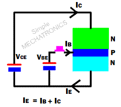
In the NPN transistor, P-type material is in between two N-type materials. Even though, both the ends are made of N-type semiconductor material, they are not interchangeable, due to difference in doping. Normally the middle P-type layer is very thin and one of the N-type layer is larger than other end. Here larger layer is called as Collector and other end is called as Emitter. The middle thin P-type layer is called as Base.


The two voltage sources (VBE and VCE), required for proper working of an NPN transistor is shown here. Very small current flow through the Base (IB) due to VBE, makes the lower PN-junction, forward biased like a diode. Due to this phenomenon, majority of electrons cross the barrier between the Emitter and Collector also, which makes the current flow from Collector to Emitter in high quantity. So, with a small current flow at Base, high current flows between Collector and Emitter.
So, the total current flow at Emitter is sum of Current flow through the Base and Collector.
For practical use, NPN transistor is configured as either Common Emitter or Common Collector mode. The power source is connected between the Collector and Emitter and signal (low current and voltage input) is applied at Base pin. The effect of signal in both the configurations are shown below. Resistors are to be used to control the current flow through the Collector, Emitter and Base as required, which is dependent on its design parameters (available in data sheets of the particular transistor)


PNP Transistor:

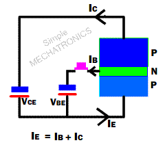
Where as in the PNP transistor, N-type material is in between two P-type materials. Like NPN, both the ends (P-type) are not interchangeable, due to difference in doping. Here the middle N-type layer is very thin and one of the P-type layer is larger than other end. Here also, larger layer is called as Collector and other end is called as Emitter. The middle thin P-type layer is called as Base.

For the PNP transistor also, the two voltage sources (VBE and VCE), required for proper working, as shown here. Very small current flow through the Base (IB) due to VBE, makes the lower PN-junction, forward biased, and due to this phenomenon, majority of electrons cross the barrier between the Emitter and Collector also, which makes the current flow from Emitter to Collector in high quantity. So, with a small current flow at Base, high current flows between Collector and Emitter.
So, here also the total current flow at Emitter is sum of Current flow through the Base and Collector. The main difference w.r.t. NPN is, the Emitter should be connected towards positive supply and Collector to negative supply.
For practical use, PNP transistors also configured as either Common Emitter or Common Collector mode. The power source is connected between the Collector and Emitter and signal (low current and voltage input) is applied at Base pin. The effect of signal in both the configurations are shown below. Resistors are to be used to control the current flow through the Collector, Emitter and Base as required, which is dependent on its design parameters (available in data sheets of the particular transistor)


The NPN and PNP transistors are highly used as signal amplifiers and logic gates. The ratio of current flow at Collector to Base is called Gain of the transistor, which is always greater than 1 (typically 100).
Field-Effect Transistor (FET):
A Field Effect Transistor (FET), (also called Uni-polar Device / Transistor), is different from normal Bi-polar Junction Transistor (BJT) in construction and working principle. A BJT (eg NPN or PNP) is current controlled device, which responds to current flow through its base. Where as an FET is voltage controlled device, which responds to the voltage at gate pin w.r.t. source pin, so has very input resistance. Due to its construction and working principle, the FET's are classifed as Junction Field Effect Transistors (JFET) and Metal Oxide Semiconductor Filed Effect Transistor (MOSFET).
Junction Field-Effect Transistor (JFET):
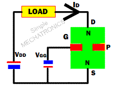
Junction Field Effect Transistor (JFET), are two types based on the semiconductors used for construction. i.e., n-channel JFET and p-channel JFET, which is depending on the main and control semiconductors used for construction. Both the types of JFETs are shown here.


A JFET is operated in reverse biased, between the Gate and Source pins for control. So, when the voltage increases at PN-junction, between the Gate and Source, the Reverse-bias reduces / prevents the current flow (ID) through the Drain pin. Higher the reverse bias voltage causes, higher the resistance (i.e., lower the current) between the source to drain. The working system of n-channel JFET is shown here. The polarity of power supply is reversed for p-channel JFET.
Metal Oxide Semicondictor Field-Effect Transistor (MOSFET):
Metal Oxide Semicondictor Field Effect Transistor (MOSFET) is also called as Insulated Gate Field Effect Transistor (IGFET). The MOSFET does not have PN-junction like JFET, but controlled by P type or N type channel The channel is controlled by a Silicon Dioxide (SiO2) layer. The MOSFET is sub-divided into Depletion type MOSFET (D-MOSFET) and Enhancement type MOSFET (E-MOSFET). The working principle and differences of D-MOSFET and E-MOSFET are explained below.
Depletion type MOSFET (D-MOSFET):
The D-MOSFET, either n-type or p-type semi-conducting material, is diffused to source and drain, which is connected by a narrow channel of same material. The remaining gap is filled with the opposite (p-type or n-type) semi-conductor. A Silicon-dioxide layer is used at the channel area, which is connected to the gate.


When the gate is connected in reverse biased w.r.t. source, the width of the channel near gate (which is connected to SiO2), increases and reduces the flow of current between source and drain. So, the current flow between source to drain is inversely proportional to gate voltage.
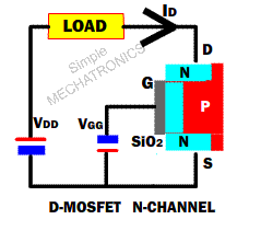
In case, the gate is connected in forward biased w.r.t. source, then the width of the channel increases and more current flows from source to drain, which is called as enhancement mode and it is very rarely used on D-MOSFET.
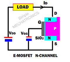
Enhansement type MOSFET (E-MOSFET):
The E-MOSFET, either n-type or p-type semi-conducting material, is diffused to source and drain and there is no connection between them, except a Silicon Dioxide (SiO2) layer connected to the gate pin. The gap is filled with the opposite (p-type or n-type) semi-conductor.


When the gate is connected in forward biased w.r.t. source, a channel is created to connected the semiconductors of source and drain, which allows current flow between the source and drain. The width of the channel near gate (which is connected to SiO2), increases with more forward biased voltage, which in turn increases the flow of current between source and drain. So, the current flow between source to drain is directly proportional to gate voltage.
Transistor Packages:
Transistors are available in various packages, depends on current flow, maxiumum power and response speed (in MHz). Some of the commonly available packages are listed here.
TO-3, TO-18, TO-92, TO-220, TO-220AB, TO-226, SOT-32 etc.
Transistor Revolution is origin for Modern electronics, Micro-controllers and Computers.
– Simple Mechatronics